Intel Museum
Somewhere inside the building, behind glass, sits the original IBM PC -- the machine that brought computing out of the mainframe room and into the American living room. The Intel 8088 microprocessor inside it contained 29,000 transistors. Today, an Intel chip smaller than your thumbnail holds billions. The Intel Museum, tucked into the ground floor of the company's Santa Clara headquarters, tells the story of that exponential leap, and it does so for free, to anyone who walks through the door.
From Internal Archive to Public Showcase
The museum began in the early 1980s as an internal project -- Intel employees collecting artifacts from a company that was barely fifteen years old but already reshaping the world. Circuit boards, engineering notebooks, early chip prototypes: the kind of ephemera that companies usually discard, Intel's archivists preserved. By 1992, the collection had grown significant enough to open to the public on February 13 of that year, a modest gallery in the lobby of a semiconductor giant. Seven years later, in 1999, Intel tripled the exhibition space and added a retail store. The expansion reflected a shift in Intel's relationship with the public. This was no longer just a chipmaker selling to other businesses; after the wildly successful Intel Inside campaign of the 1990s, it was a consumer brand, and the museum became its most tangible point of contact with ordinary people. Open weekdays except holidays, it charges no admission -- a deliberate choice that keeps the doors open to anyone curious enough to walk in.
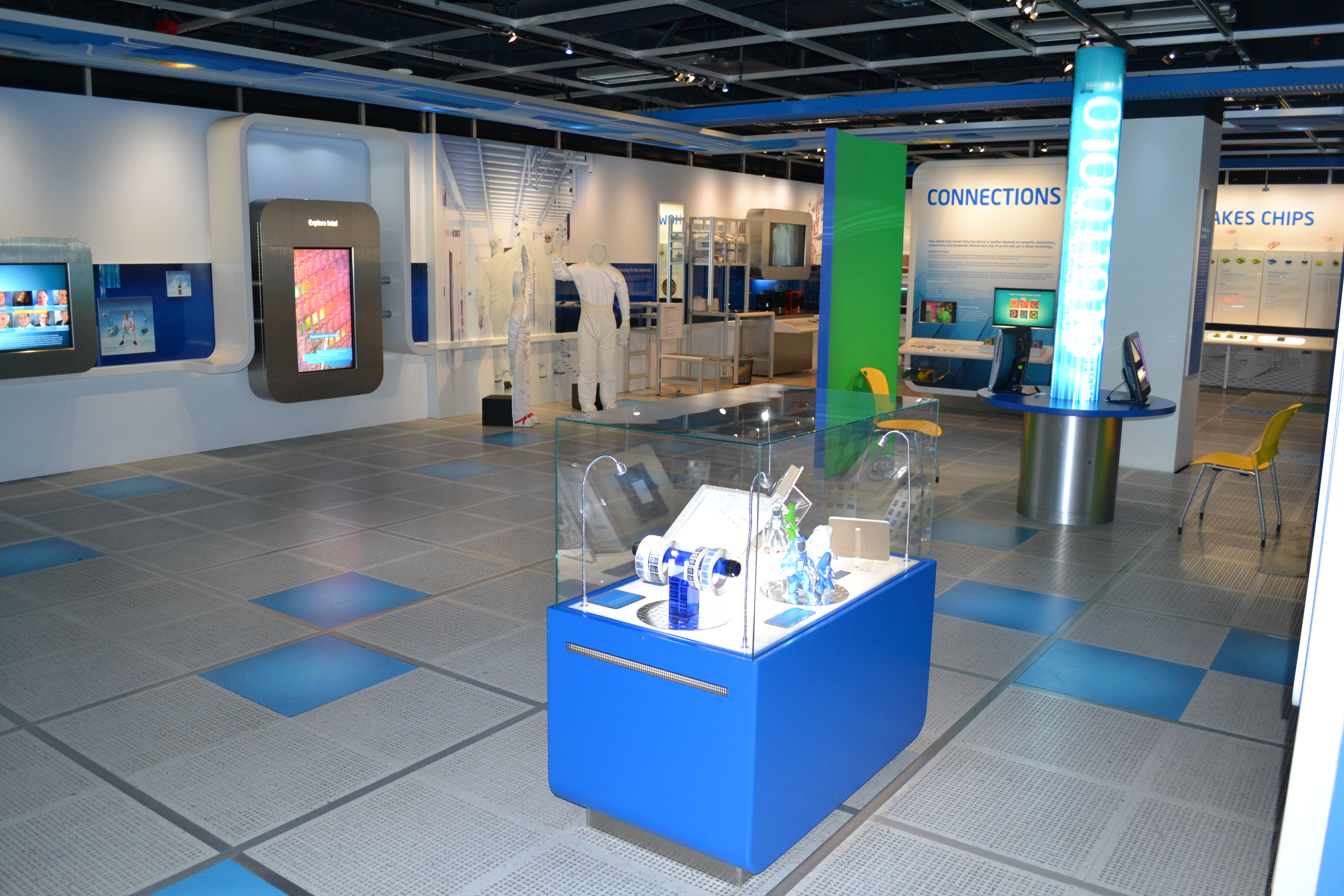
Sand to Silicon
The centerpiece of the museum is not a single artifact but a process. Exhibits walk visitors through the journey from raw silicon to finished microprocessor -- how sand is refined into crystalline ingots, sliced into wafers, etched with circuit patterns measured in nanometers, and packaged into the chips that drive everything from laptops to data centers. A scale model of a semiconductor fabrication plant reveals the cathedral-like clean rooms where workers in bunny suits handle wafers worth thousands of dollars apiece. The air inside a real fab is cleaner than a hospital operating room; a single speck of dust can ruin a chip. Silicon ingots and wafers of increasing size sit on display, a physical timeline of the industry's growth. The largest wafers, 300 millimeters across, dwarf the early discs from the 1970s. Stand in front of the exhibit long enough and the sheer improbability of the enterprise sinks in: turning beach sand into a thinking machine, billions of transistors at a time.
The People Behind the Processors
An exhibition devoted to Robert Noyce, co-founder of Intel and co-inventor of the integrated circuit, anchors the museum's historical wing. Noyce and Gordon Moore left Fairchild Semiconductor in 1968 to start Intel, naming the company for "Integrated Electronics" after rejecting "Moore Noyce" -- a near-homophone for "more noise," hardly ideal for an electronics firm. Their third employee was Andy Grove, the Hungarian-born chemical engineer who would drive Intel's ferocious growth through the 1980s and 1990s. A nearby exhibit on Moore's Law -- Gordon Moore's 1965 observation that the number of transistors on a chip doubles roughly every two years -- shows how that prediction held for decades and became the metronome of an entire industry.
Learning by Doing
The museum doubles as a classroom. Self-paced exhibits let visitors design a virtual chip, test transistor logic, and explore the physics of semiconductor doping. Grade-school groups can book guided educational programs that break down chip fabrication into steps a ten-year-old can follow. It is a deliberate strategy: Intel has long understood that today's curious fourth-grader is tomorrow's electrical engineer. The exhibits avoid jargon where they can, favoring interactive models and tactile demonstrations over text-heavy panels. For a subject as abstract as integrated-circuit design, the approach works -- you leave understanding, at least in broad strokes, how the device in your pocket was built. In a valley where billion-dollar companies guard their campuses behind badge readers and security gates, the Intel Museum remains one of the few places where the public can walk inside the industry that shaped the modern world and see, up close, how it actually works.
From the Air
Located at 37.39N, 121.96W in Santa Clara, California, within the Intel headquarters campus along Mission College Boulevard. The large corporate campus is identifiable by its blue-glass office buildings adjacent to the Great America Parkway corridor. Nearest airports: San Jose International (KSJC, 3nm S), Moffett Federal Airfield (KNUQ, 4nm NW), Palo Alto (KPAO, 8nm NW). Best viewed at 2,000-3,000 feet AGL to see the campus layout amid the sprawl of Silicon Valley office parks.